First we must consider these imperfect amplifiers.
The later feedback and precision circuits would be useless without them!
- The fraction of the electrons leaving the emitter and going to the collector
instead of the base is normally called
[(Icollector)/( Iemitter)] = a.
More strictly, in case of non-linear behaviour, we define
a = [(dIcollector)/( dIemitter)]
-
The ratio of the collector current to the base current is normally called
b.
Thus,
b = [(Icollector)/( Ibase)]
From this we can get
b = [(a)/( 1-a)].
More strictly, in case of non-linear behaviour, we define
a = [(dIcollector)/( dIemitter)]
-
Hence
(1-a)b = a
a = [(b)/( 1+b)]
-
By arranging the geometry so that the base region is very thin,
most of the electrons entering from the emitter into the base will
be fall over the edge down the steep electric potential fall of the
base-collector junction before they meet and recombine with holes in the base.
Thus, by making the base be very thin so that the emitter-base junction
and the collector-base junction are very close,
and doping the collector-base junction so that it is very thin (with a high
electric field [E\vec] = -[dV/ dx], the fraction a
of the electrons leaving the emitter and going to the collector
instead of the base can be made close to 1.0 and
b = [(a)/( 1-a)] can be made large.
This can make the transistor more useful.
While a transistor with a large b, such as
b = 100, can be used
to make amplifiers with a high gain, the thin base and collector-base junction
have a general defect.
This defect is that the thin collector-base junction will have high electric
fields [E\vec] and avalanche breakdown may occur.
-
So long as the collector-base voltage is greater than about 2 or 3 volts,
very few of the electrons which fall over the collector-base junction
can bounce back.
Thus, So long as the collector-base voltage is greater than about 2 or 3 volts,
the fraction a of electrons passing through both
junctions is only slightly dependent upon the collector-base voltage.
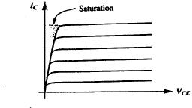
A typical set of Icollector and VCollector-Emitter curves for
equispaced base currents are shown below.
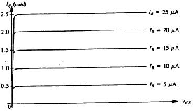
Although the following curves are not usually shown in specifications,
the following shows ICollector and IBase curves for equispaced
collector voltages.
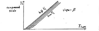
- Thus a and particularly b are useful parameters because they are
nearly constant for any given bipolar junction transistor over a range
of working voltages and currents.
The b may vary from one transistor to another due to manufacturing
variations and due to changing temperature.
Note that IC in the following graph has a logarithmic horizontal scale
and covers a very wide rage.
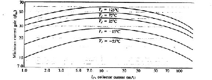
Even though b does not change much with voltage and current, in any
given transistor, the variation in b due to temperature and manufacturing
is significant.
The variation due to manufacturing, can be minimized by selecting transistors
with particular values of b.
-
In most practical circuits, we try to make the
action be independent of b.
This can be done in a variety of ways but will require that b be large
so that b >> 1 and we can approximate functions like b+1 as b.
-
The transistor is said to be in saturation if the collector voltage is too low.
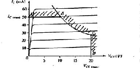
- Any transistor has maximum ratings for
- The maximum power giving a maximum product of IC max and
VCE max.
-
A maximum current into the collector IC max through its connecting
wire and weld.
-
A maximum voltage on the collector-base junction VCE max above which the
junction may break down.
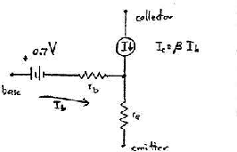
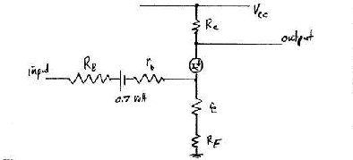
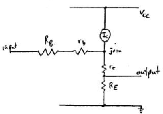
We want a 3-terminal model which we can use to ``replace the transistor''
when want to make calculations.
In this model we assume
A common convention is to use lower case r for each of the internal
resistances to distinguish them from the normal external resistors
we attach to the emitter, base and collector.
We replace the base to emitter junction with a small 0.7 volt battery with a
small (perhaps negligible resistor rb.
From the previous discussion of p,n junctions, we know
that the emitter has the dynamic junction impedance (which may also be negligible)
of about
re = 2 ohm + [0.026 volt/( Ibase)].
- Grounded Emitter Amplifier
The simple transistor model suggests how an amplifier might be made.
We call this a grounded emitter amplifier.
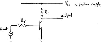
Variations DVinput in the base input voltage will cause
variations in the emitter current
through rb.
The transistor can be replaced for calculation purposes by the
transistor model as in the next diagram.
If, as usual, re is small, then
DIb = [(DVinput)/( RB+rb)]
and these will cause variations in the collector current
DIc = bDIb = b [(DVinput)/( RB+rb)]
The changing collector current flows through the collector resistor Rc
from a constant voltage usually called ``Vcc'' and so the changing
collector current causes the collector voltage to change by
DVC = - RC b [(DVinput)/( RB+rb)]
DVC = -([( RC b )/( RB+rb)]).DVinput
Thus a small change in the input to the base can cause a larger change
in the voltage of the collector.
- The ``voltage gain'' or ``amplification''
[(Vc)/( Vb)] = -([( RC b )/( RB+rb)]) is
negative meaning that the output signal is inverted relative to the
input signal. This is not an disadvantage but is actually an advantage
for negative feedback and for digital circuitry.
- This circuit is very easy to understand but is seldom used for
the following reasons.
- It is hard to make transistors with a particular precise value of b.
- In any transistor, b depends upon temperature
- b also depends, slightly, upon the collector voltage and collector
current Ic. (In other words, the transistor model is not very precise.)
- rb depends, a little, upon temperature, Ib and Ic.
- re depends, a little, upon temperature, Ib and Ic.
- The voltage difference across the junction (near 0.7 volt) is
temperature dependent.
In general, the grounded emitter gives a high amplification but the voltage
gain [(Vc)/( Vb)] is too unpredictable for this circuit to be used
except in digital circuits.
The following three amplifying circuits include some type of
``negative feedback'' to overcome these problems.
Other circuits use transistors in identical pairs and use them
to amplify pairs of voltages (one the signal and the other a constant voltage
or a negative signal) so that some of the unwanted effects can cancel.
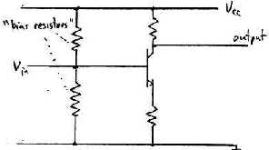
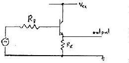
- Common Emitter Amplifier
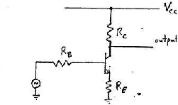
This has 3 resistors as shown RB, RE and RC attached to
the base, emitter and collector.
The top ``rail'' is attached to a positive power supply (perhaps +10 Volt).
The lower ``rail'' is the ground.
The input is on the left (via the resistor RB. The output is on the
right from the collector pin attached to the resistor RC.
Apply a small incremental voltage DVin to the resistor RB
leading to the base.
The transistor can be replaced for calculation purposes by the
transistor model as in the next diagram.
We concern ourselves only with the current and voltage increments so can
ignore the +0.7 volt battery.
Define the voltage on the point below the current generator at the join
of the 3 lines as DVjoin
We can obtain 2 equations.
- The current increment DIBase into the base due to the voltage
increment DVin is
DIBase = [(DVin-DVjoin)/( RB+rb)]
- The current increment DICollector into the Collector due to the voltage
increment DVin is
DICollector = bDIBase
The voltage increment across the actual resistor RE and the
internal resistance re totalling
RE+re, due to the two currents caused by
the voltage increment DVin is
DVjoin = (1+b)DIBase(RE+re)
From these two equations
DIBase = [(DVin- (1+b)DIBase(RE+re))/( RB+rb)]
(RB+rb)DIBase = DVin- (1+b)DIBase(RE+re)
(RB+rb)DIBase + (1+b)DIBase(RE+re) = DVin
(RB+rb + (1+b)(RE+re))DIBase = DVin
DIBase = [( DVin)/( (RB+rb + (1+b)(RE+re)))]
From this, we can calculate 3 important parameters for this circuit.
- The Voltage Gain of the common emitter circuit
The collector voltage will decrement due to the increased current through
the resistor RC from the positive +10 Volt supply.
Thus the voltage increment on the collector will be negative;
DVC = -DICRC
DVC = -bDIBaseRC
DVC = -b[(DVin)/( (RB+rb + (1+b)(RE+re)))]RC
Thus the voltage gain of this common emitter circuit is
AV = [(DVC)/( DVin)] = -[(bRC)/( (RB+rb + (1+b)(RE+re)))]
If we neglect both rb and re, then
AV » -[(b(RC))/( (RC + (1+b)RE))]
again, if we assume that b >> 1, the voltage gain, AV, becomes
AV » -[(RC)/( RE)]
Notes.
- The gain is negative meaning that the output voltage signal is inverted.
-
Using the concepts of feedback, we say that the resistor RE is providing
negative feedback so that in the approximations of b being high and
rb and re being low,
the voltage gain AV is
minus(the ratio of the collector and emitter resistances)
- The Input Impedance of the common emitter circuit
The Input Impedance is the ratio
Zin = [(DVin)/( DIBase)]
Use DIBase from above
Zin = (RB+rb + (1+b)(RE+re))
Again, if we neglect rb and re and assume that
b >> [(RB)/( RE)]
then
Zin = bRE
- The Output Impedance of the common emitter circuit
Remembering that the impedance of a current generator is infinite, the output
impedance of the circuit looking back into the circuit is only that of the
resistor RC to the power supply which is a virtual ground.
Thus we have
Zout = RC
- Common Collector Amplifier (The ``Emitter Follower'')
This has 2 resistors as shown RB and RE attached to
the base and emitter.
The top ``rail'' is attached to a positive power supply (perhaps +10 Volt).
The lower ``rail'' is the ground.
The Collector is attached directly to the top rail at +10 Volt.
The input is on the left (via the resistor RB. The output is on the
right from the emitter pin attached to the resistor RE.
Apply a small incremental voltage vin to the resistor RB leading
to the base.
The transistor can be replaced for calculation purposes by the
transistor model.
Apply a small incremental voltage DVin to the resistor RB
leading to the base.
We concern ourselves only with the current and voltage increments so can
ignore the +0.7 volt battery.
Define the voltage on the point below the current generator at the join
of the 3 lines as DVjoin
As with the Common Emitter before, we can obtain 2 equations.
- The current increment DIBase into the base due to the voltage
increment DVin is
DIBase = [(DVin-DVjoin)/( RB+rb)]
- The current increment DICollector into the Collector due to the voltage
increment DVin is
DICollector = bDIBase
The voltage increment across the actual resistor RE and the
internal resistance re totalling
RE+re, due to the two currents caused by
the voltage increment DVin is
DVjoin = (1+b)DIBase(RE+re)
From these two equations
DIBase = [(DVin- (1+b)DIBaseRE)/( RB+rb)]
(RB+rb)DIBase = DVin- (1+b)DIBase(RE+re)
(RB+rb)DIBase + (1+b)DIBase(RE+re) = DVin
(RB+rb + (1+b)(RE+re)DIBase = DVin
DIBase = [( DVin)/( (RB+rb + (1+b)(RE+re)))]
From this, we can calculate 3 important parameters for this circuit.
- The Voltage Gain of the common collector (emitter follower) circuit
The current through the emitter is
DIEmitter = (1+b)DIBase
The voltage increment across RE is the output signal DVout
DVout = DIEmitter RE
DVout = (1+b)[( DVin)/( (RB+rb + (1+b)(RE+re)))] RE
DVout = [((1+b)RE)/( (RB+rb + (1+b)(RE+re)))]DVin
If we neglect re and rb
DVout » [((1+b)RE)/( (RB + (1+b)RE))]DVin
If b >> 1, then
DVout » [((1+b)RE)/( (RB + (1+b)RE))]DVin
The voltage Gain
AV = [(DVout)/( DVin)] » [((1+b)RE)/( (RB + (1+b)(RE)))]
If (RB << (1+b)RE then
AV = 1.0
-
The Input Impedance of the common collector (emitter follower) circuit
The Input Impedance is the ratio
Zin = [(DVin)/( DIBase)]
Use DIBase from above
Zin = (RB+rb + (1+b)(RE+re))
Again, if we neglect rb and re and assume that
b >> [(RB)/( RE)]
then
Zin = bRE
- The Output Impedance of the common collector (emitter follower) circuit
To calculate this, we assume no change to Vin (ie DVin = 0) but
draw a small current DIout from the output
(emitter pin) and calculate or measure the resulting DVout.
We concern ourselves only with the current and voltage increments so can
ignore the +0.7 volt battery.
Again, define the voltage on the point below the current generator at the join
of the 3 lines as DVjoin
As with the Common Emitter before, we can obtain 2 equations.
- DVjoin = -DIbase(RB+rb
-
Vjoin = (b+1)DIbase re + ((1+b)DIbase-DIout)RE
-DIbase(RB+rb = (b+1)DIbase re + ((1+b)DIbase-DIout)RE
Grouping the Ibase terms on the right
DIoutRE = DIbase[RB+rb+(1+b)(re+RE)]
DIbase = [(DIoutRE)/( [RB+rb+(1+b)(re+RE)])]
The change in the output voltage DVout is due to the two changes
in current through RE
DVout = ((increase in emitter current)-(current drawn from output))RE
DVout = ((1+b)DIbase-DIout)RE
DVout = ((1+b)[(DIoutRE)/( [RB+rb+(1+b)(re+RE)])] -DIout)RE
The Output impedance is
Zout = -[(DVout)/( DIout)] = -(1+b)[(RE2)/( [RB+rb+(1+b)(re+RE)])] +RE
Zout = -(1+b)[(RE2)/( [RB+rb+(1+b)(re+RE)])] +RE
Zout = -[((1+b)RE2)/( [RB+rb+(1+b)(re+RE)])] +RE
Zout = [(-(1+b)RE2+[RB+rb+(1+b)(re+RE)]RE)/( [RB+rb+(1+b)(re+RE)])]
Zout = [(+[RB+rb+(1+b)(re)]RE)/( [RB+rb+(1+b)(re+RE)])]
If rb and re are very small
Zout = [(RBRE)/( [RB+(1+b)RE])]
If b is large
Zout = [(RB)/( 1+b)]
The output impedance has been lowered to a fraction [1/( 1+b)] of
the RB. In this way, an emitter follower (common collector circuit)
can be used to lower the effective output impedance of any device which
might have had an output impedance of RE.
The emitter follower (common collector) circuit is often used together with
another circuit which might already provide sufficient voltage gain.
- Common Base
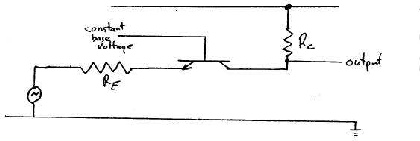
This has 2 resistors as shown RE and RC attached to
the emitter and collector.
The top ``rail'' is attached to a positive power supply (perhaps +10 Volt).
The lower ``rail'' is the ground.
The Base is attached directly to a constant voltage, say +3.0 volt and so can
act as a common reference point for both the input side and the output side.
Define the voltage on the point below the current generator at the join
of the 3 lines as DVjoin.
Define the voltage on the point X below the current generator
as DVX.
The transistor can be replaced for calculation purposes by the
transistor model as in the next diagram.
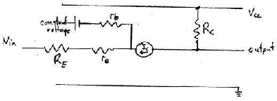
We will later apply a small incremental voltage DIin to the point X between the
resistor RE and the emitter.
- First, however, consider the circuit with no inputs signals
(ie DIin = 0).
The Transistor Model gives us the equivalent circuit for incremental voltages
and currents.
If Vb = +3.0 volt, then
|
Vjoin = +3.0 volt-0.7 volt-rbIb |
| (1) |
The current through the resistor RE and internal resistance re
is IC+Ib = (b+ 1)Ib
The voltage at point ``join'' is
Vjoin = (IC+Ib)(re+RE)
|
VC = 10 volt -ICRC = 10 volt -(b+1)IbRC |
| (3) |
Use equations 1 and 2 to eliminate Vjoin.
2.7 volt - rbIb = (b+ 1)Ib(re+RE)
Ib = [2.7 volt/( rb+(b+1)(re+RE))]
Substitute this Ib into equation 3.
|
VC = 10 volt-(b+1) |
2.7 volt
rb+(b+1)(re+RE)
|
RC |
| (4) |
--------
- Now calculate these again but with the addition of an input current Iin due
to the signal introduced via a capacitor.
Consider the circuit with an injected input current signal,
DIin = 0.
The Transistor Model gives us the equivalent circuit for incremental voltages
and currents.
Calculate the new values for Vjoin, IC, Ib, and VC.
If Vb = +3.0 volt, then
|
Vjoin = +3.0 volt-0.7 volt-rbIb |
| (5) |
The current through internal resistance re
is IC+Ib = (b+ 1)Ib.
However the current through the resistor RE will differ due to
the input signal.
The voltage at point ``join'' is
Vjoin = (IC+Ib)re+(IC+Ib+DIin)RE
|
Vjoin = ((b+1)Ib)re+((b+1)Ib+DIin)RE |
| (6) |
|
VC = 10 volt -ICRC = 10 volt -(b+1)IbRC |
| (7) |
Use equations 5 and 6 to eliminate Vjoin.
2.7 volt - rbIb = ((b+1)Ib)re+((b+1)Ib+DIin)RE
This can be simplified
2.7 volt-DIinRE = (rb+(b+1)(re+RE))Ib
Ib = [(2.7 volt-DIinRE)/( rb+(b+1)(re+RE))]
Substitute this Ib into equation 7.
|
VC = 10 volt-(b+1) |
2.7 volt-DIinRE
rb+(b+1)(re+RE)
|
RC |
| (8) |
Compare this equation 8 with the previous equation 4.
The injected input current DIin has changed the output voltage
by
|
DVout = New VC- Old VC = (b+1) |
DIinRE
rb+(b+1)(re+RE)
|
RC |
| (9) |
If re and rb are small,
|
DVout » (b+1) |
DIinRE
(b+1)(RE)
|
RC |
| (10) |
Note
From this, as before we can calculate 3 important parameters for this circuit.
- The Voltage Gain of the common base circuit
-
The Input Impedance of the common base circuit
-
The Output Impedance of the common base circuit
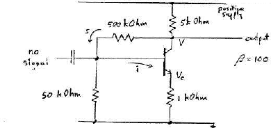
Often, these two conditions imply that the bias resistors must be kept between
two limits which are a factor of about b apart.
For example, if b is about
b = 65, then choose bias resistors giving
the following.