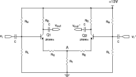
Read Horowitz & Hill (2nd Ed) page 98. That description is for a DC coupled difference amplifier using +15 volt and -15 Volt power supplies. Our amplifier is for AC signals, and uses only one power supply but we use the same notation.
If a linear amplifier has two receiving input voltages vi and vió, then its output may be a linear combination of the two inputs:
vout = X.vi +Y.vió
where X and Y are two constants. We can manipulate this equation to give
vout = [((X-Y))/ 2].(vi-vió) +(X+Y).[((vi+vió))/ 2].
In other words, vout can be written as the linear combination of the difference (vi-vió) and common mode or average [((vi+vió))/ 2].
The difference amplifier provides a number of advantages which make it one of the most useful circuit configurations, particularly as an input stage for high gain and DC amplifiers. By choosing matched transistors, often on the same piece of silicon of an integrated circuit, very stable and drift free operation may be obtained because of the symmetry of the amplifier. The differential input is particularly useful in cases where the desired signal is the difference between the voltages on two wires, which might be masked by a large and varying voltage, with respect to ground, that is common to both wires. Operational amplifiers often consist of a cascaded series of difference amplifiers which provide excellent stability and high gain. An ideal difference amplifier has a large gain for difference mode signals (vi = - vió), and zero gain for common mode signals (vi = vió). We may write the output voltage (taken from either collector) for a real difference amplifier as:
|
If one uses only a difference mode signal (ie vc = 0), then Ad = v░/vd. For the common mode signal only (vd = 0), the common mode gain can be measured Ac = vo/vc.
A figure of merit for real difference amplifiers is called the Common Mode Rejection Ratio, CMRR, which is defined as:
|
For an ideal difference amplifier, CMRR would be infinite since Ac = 0, and for real amplifiers we want CMRR as large as possible. Consider the circuit shown in Figure 1. In the calculation sheet the gains and CMRR are derived and the results are:
|
|
|
[Sometimes, in technical books, this is carelessly given with inconsistent units as rtr = @ 25/Ic(mA) + 2 ohm. Please do not use this notation.]
It is apparent that CMRR will become larger as R1 becomes larger. The large R1 acts as a current source and an active current source, using an additional transistor is often used when a very large CMRR is desired. The effect of R1 may be understood by noting that, in the difference mode the currents in the two transistors are 180░ out of phase, resulting in zero net AC current through R1, thus making point A an AC ground (a virtual ground). This means a large difference mode gain. In the common mode, however, twice the AC current flows through R1 than through one transistor. In this case it appears that there is a resistor of value 2R1 to ground and the common mode gain dramatically decreases. (For a true current source, the effective value of R1 «ź, giving Ac ~ 0.)
This writeup contains a worksheet which will enable you to calculate the component values for the circuit. This must be done before the lab session.
Refer to the difference amplifier circuit of Fig. 1. An AC equivalent circuit can be used to calculate the gains. To simplify the algebra we define Rf = rtr+RE. The gains and CMRR, which were derived before, can be rewritten:
|
|
|
Two current generators deliver currents i = bib and ió = bibó and we assume that b is large so that the base currents ib and ibó can be neglected and the emitter currents can regarded as equal to the collector currents ic and icó. Note that the inputs (the base connections) determine the voltages at the outer ends of the Rf resistors but do not supply an appreciable fraction of the current through them. (The base currents are only [1/( b)] of the collector currents.)
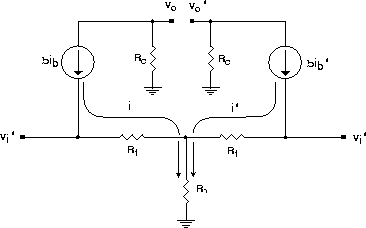
We can get 4 equations by applying ohm's law to this equivalent circuit.
| (1) |
| (2) |
| (3) |
| (4) |
A little algebra can be done on the 4 equations above to get them into the
form
vo = Ad(vi-vió) + Ac(vi+vió)/2.
Start with equation 1 minus equation 2 :
| (5) |
| (6) |
| (7) |
Substituting equation 6 :
| (8) |
Equation 1 plus equation 2 gives:
| (9) |
| (10) |
Equation 3 plus equation 4 gives:
| (11) |
Substituting equation 10 :
| (12) |
| (13) |
| (14) |
We can define vd = (vi-vói) as the ``Difference Mode'' input voltage and define vc = [((vi+vói))/ 2] as the ``Common Mode'' input voltage.
Then equation 14 becomes
| (15) |
| (16) |
where
Ad = [(RC)/( 2Rf)] is the ``Difference mode gain'' and Ac = [(RC)/( 2R1+Rf)] is the ``Common mode gain''.
We want to meet the 5 following goals for the desired operating characteristics of the amplifier. Here we have picked a set of parameters for the design.
We want the Output impedance to be Zout = 1k.
We want the Output Swing to be ▒2 V.
(We define the ``Output Swing'' as the maximum voltage excursion which can be generated on each of the outputs without the amplifier becoming non-linear. The Output Swing of 2 V means we would like the output vo to be able to change by ▒ 2 V and the output voó to be able to change by ▒ 2 V with the outputs changing in opposite directions. Each output can change from its Q Point value by +2 V to -2 V, a difference of 4 V. We say that the ``peak to peak voltage'' is vp-p = Dvc = 4 V. Thus each transistor must be able to operate in linear mode while its collector changes over a total range of 4 V.)
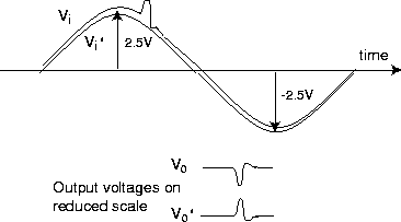
We want the common mode gain Ac to be as low as possible, consistant with a common mode input range of ▒ 2.5 V. That is, the ▒ 2 V output swing should be available when the inputs are both 2.5 V higher or lower than the ``Q-point''. For example, if the two inputs are as shown, a difference amplifier will amplify the difference with a large gain and the average with small gain Ac.
is called the ``Operating Point'' or ``Quiescent Point'' or ``Q Point''. The design choices to meet these goals are calculated below. You should follow this outline, make any necessary or suggested calculations and fill in the values in the next section.
then, later in item , calculating the bias resistors RH and RL for each base
Since RC = 1 k and we want a 2 V output swing, we adopt the static current (ie average or DC current or quiescent) through each collector to be IC = 2 mA. The collector current of each transistor can then swing 2 mA between 0 mA and 4 mA.
We can choose Rf to get the desired Difference Mode voltage Gain Ad = 8.
Since Rf = rtr+RE, RE should be about (62.5 - 14.5) ohm ╗ 47 ohm.
|
Therefore we would like to make R1 as large as practical. However, we must be careful to ensure the transistor remains in a linear mode and, for this, has vc > vtr+0.5 volt.
The output swing of +2 V requires VC = 13 V at the Q point. From the symmetry of the circuit, we can see that vE remains constant for a pure differential mode input.
Therefore to get a downward 2 V swing, vC needs to go to 11 V and vE should be no higher than 10.5 V to avoid saturation. vE follows vi, so when the input common mode voltage goes to +2.5 V, vE will be 2.5 V above the Q point.
The drop across RE is only 2 mA×47 ohms ╗ 0.1 V, so we want vA Ż 8 V at the Q point. Since the Q point current in R1 is 4 mA, R1 = [8 volt/ 4 mA] ╗ 2 k. However, our 10% resistors have standard values of 1.0, 1.2, 1.5, 1.8, 2.2. 2.7, with any multiplier, so we choose the nearest standard value of resistor on the low side which is 1.8 k.
VB = ____________ V.
VBó = ____________ V. VE = ____________ V.
VEó = ____________ V. VA = ____________ V. VC = ____________ V.
VCó = ____________ V.
The bias network must now supply the appropriate VB.
We have a voltage for VB of
VE = 4 mA× 1.8 K (about 0.1 V across RE) +0.7 V ╗ 8 V.
This gives the required ratio for RH and RL assuming that
b«ź.
To allow for bmin = 75, we must limit the Thevenin impedance of the voltage divider. If we want the maximum change in the emitter Q point to be 0.2 V, then IB =2 mA/75 through the Thevenin impedance must produce a voltage drop of less than 0.2 V.
Use these values to calculate RH and RL and then choose the closest available values from the list of standard resistor values. RH = ____________ ohm
RL = ____________ ohm Calculate the expected Ac and Ad using the actual resistor values. Ac = ____________
Ad = ____________