Physics 623
Physics 623
Digital Circuits I and II
Nov 17, 1999
Digital Circuits I
1 Purpose
- To introduce the basic principles of digital circuitry.
- To understand the small signal response of various gates and
circuits typical of the currently available TTL integrated circuitry.
2 Discussion
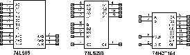
The circuits are TTL 7400 series of various types from various manufacturers.
Use the built-in supply for Vcc = +5 V DC.
The logic levels are:
- One: 3 to 5.0 volts; nominally 4.75 V.
- Zero: 0 to 0.4 volts; nominally ground = 0 V.
- Switching Level ~ 1.4 V.
The delay in passing a signal through one NAND gate is typically 13 ns
for the SN7400 series and is about 7 ns for the 74LS00 series.
The fanout capability is 10, (i.e. ten inputs can be connected to each
output). The operating temperature range is from about 0°C to
70°C. The general characteristics of TTL logic are described in the
attached sheets together with the detailed specifications of individual chips.
3 Procedure
- Verify the truth table for a two input NAND gate.
|
|
| A | B | Y |
|
|
| 0 | 0 | 1
|
| 0 | 1 | 1
|
| 1 | 0 | 1
|
| 1 | 1 | 0 |
- Use 2 input NAND gates to implement the logic values shown below.
Use DeMorgan's theorem, if necessary. Use the switches and/or push buttons on
your breadboard for inputs and the LED indicators to show the output states.
- (a)
-
A 2 input AND gate.
Y = A ·B
- (b)
-
A 2 input exclusive OR
Y = A ĹB or equivalently
Y = A ·[`B] + [`A] ·B
- (c)
-
Show the circuit -(don't build)
Y = (A ·B ·C) + D + E
- Cross couple 2 NAND gates to make an RS flip-flop. Then add
the gates to make a DATA flip-flop. Test its properties.
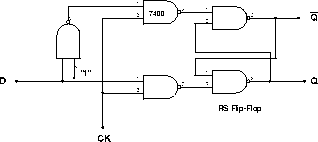
note: ``1'' means that this input should be held at the logical 1
level by connecting it to +5V.
-
Verify the truth table for a JK flip-flop, using the 74LS112.
(The Clock is CP). The data sheet for the out-dated 7473 flip-flop is included
for its superior functional block diagram. Study it and see how a JKFF works.
|
|
| J | K | Qn+1 |
|
|
| 0 | 0 | Qn
|
| 0 | 1 | 0
|
| 1 | 0 | 1
|
| 1 | 1 | [`(Qn)] |
Here, J and K refer to the respective input
levels when the nth clock is high, and Qn+1 refers
to the output after clock returns from 1 to 0. These flip-flops have
a ``set'' (SD) and a ``reset'' (RD) feature. Experiment with the [`SD] and [`RD] inputs to determine their effect. See waveforms on
pg 4-168 of the 74LS112 data sheet.
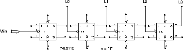
- Connect the 74LS112 JKFF's to make an 4 bit counter (0 to 15).
To display the sequence of bits use the lights on the board. Don't forget to
hook up all the inputs, even if they aren't shown on the functional logic
diagram.
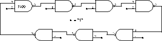
- Make a ring oscillator.
Use an odd number of gates. A signal is propagated around the loop with
a speed depending on the delay of each gate and the number of gates. For
7 gates the period is about 50 - 150 nsec., depending on the type of gate.
Check the frequency by looking at the output of any gate with the scope.
Use your four bit counter to count the oscillations.
Digital Circuits II
4 Purpose
- To continue the study of the basic principles of digital circuitry.
- To understand the operation of various special purpose gates and
circuits.
5 Discussion
The circuits are logically TTL 74LS00 series from various
manufacturers.
A reminder that the logic levels are:
- One: 3 to 5.0 V; nominally 4.75 V.
- Zero: 0 to 0.4 V; nominally ground = 0 V.
- Switching Level ~ 1.4 V.
The delay in passing a signal through one NAND gate is typically 7-13 ns.
However, depending on availability, you may be using a device which, although
it has the same voltage and logic values as normal TTL, will differ in speed and
input power required. For example ``Shottky TTL'' is distinguished by
the LS notation and is significantly faster than the normal TTL.
Some of the gates
we are using in this lab are based on CMOS technology and are pin-for-pin
compatible with TTL, denoted by the initials HCT preceding the chip number.
The fanout capability is usually 10, (i.e. ten inputs can be connected to each
output).
The detailed specifications of the individual chips are described in the
attached sheets.
6 Procedure
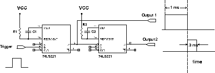
- Study the behavior of the monostable multivibrator (oneshot).
A dual oneshot has an id number 74LS221. Connect the circuit shown.
Check the spec sheet for valid resistor and capacitor values!
Arrange the two outputs so that they have the appropriate
relative timing when triggered by a rising edge. Determine the output pulse
width relative to the RC time constant of your external circuit.
What changes would have to be made to trigger your circuit on the
falling edge?
What would the result be if you used the rising-edge trigger input (B) on the
second one-shot?
- Investigate the properties of the 8 bit serial-input parallel-output
shift register (ID = 74HCT164). Connect the chip, then clock various
numbers into the register using the switches. Use the eight LED's on the
breadboard to show the states of the output. How does the ``Reset'' function
work? Keep the circuit set up for the next exercise.
-
The 74LS283 is a four bit adder which performs the binary
addition of one 4 bit number (A1 to A4) to another (B1 to B4),
including a ``carry in '' bit (C0), in order to produce a 4-bit sum
(S1 to S4) plus a ``carry out'' (C4).
Use the shift register to generate both the input binary numbers, so
that A1 to A4 correspond to QE through QH and B1 to B4 to
QA through QD. For convenience it is useful to connect the input and output
4-bit numbers to a hex display using the TIL311 chip. Verify the addition.
- Replace the adder with a four bit magnitude comparator (74LS85).
Compare the two displayed numbers and verify all the outputs.
Now experiment with the carry inputs to determine what values are required
to function correctly.
File translated from TEX by TTH, version 1.93.
On 17 Nov 1999, 19:20.