Modern integrated circuit operational amplifiers (op amps) have characteristics so closely approaching the ideal op amp that they are components of almost all signal processing and instrumentation equipment. The properties of a commonly used 741 op amp are compared to the ideal values listed in the table below:
| Parameter | Ideal Value | mA741 Value | 1990 best avail. value |
| (not all in same device) | |||
| Input current | Iin = 0 | ~ 80 nA | 0.1 pA |
| Voltage gain | Av = Ą | 200,000 | 2×10⁶ |
| Bandwidth | BW = Ą | 1 MHz at Av = 1 | 500 MHz |
| Balance | Vo = 0 for Vi = 0 | Vo = 0 at Vi = 1-2 mV | 5 mV |
| Temperature | none | (dV/dT)offset typically | (dV/dT)offset 0.1 mV/C |
| dependence | 15 mV/° C |
Op amps can be obtained commercially for $0.50 to $3.00 each. This and their versatility are the reasons for their great popularity. As you perform the suggested investigations, be alert to observe and note those cases in which the real op amp fails to match the ideal properties. Try to find the relevant properties in the ``spec sheets'', and take note of the ``typical applications'' section - this is a prime spot for getting circuit ideas or finding out how new devices might be used.
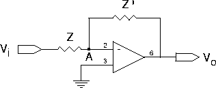
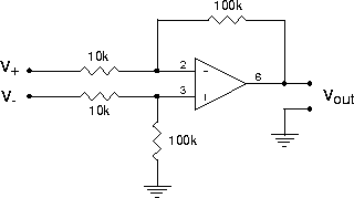
Almost all applications of op amps involve negative feedback as indicated in the diagram below:
Assume that point A is a virtual ground (i.e. V- = V+), and that Ii = 0, and prove the general result that
|
|

|
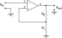
(This particular circuit has several drawbacks. Check Horowitz & Hill for a nifty ``3 Op-Amp Instrumentation Amplifier'' that has:
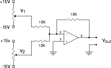
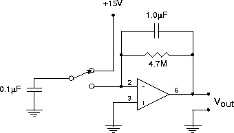
The circuit consists of three identical stages, which should be arranged from left to right across the upper breadboard block, leaving about 1/3 of the block free on the left. Clip the component leads short and bend them with your pliers so that the component bodies lie flat against the breadboard - this minimizes stray capacitances. Use a single bus on the socket for all the grounds - for example, the inner strip just below the op amps. It is a good idea to put 0.1 mF ceramic capacitors from the ± 15 V supply pins to the ground bus as close as possible to each op-amp. The instructor will show you a sample layout before you start.
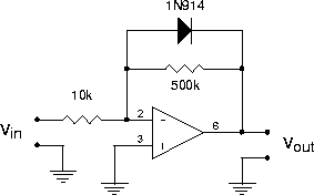
The circuit for a single tuned amplifier stage is:
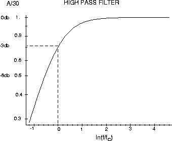
Ignoring the capacitors for a moment, this is just an inverting amplifier with a gain of RF/R1 = 30. The addition of C1 introduces a high-pass corner at f1 = 1/2pR1C1 that reduces the gain at low frequencies, ie f << f1:
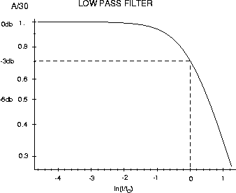
The addition of Cf reduces the gain at high frequencies, i.e. f2 = 1/2pRfCf
With both capacitors, the gain is just the product of these two curves. Since f1 = f2 ş f°, the result is :
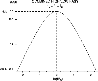
Therefore, the maximum gain of the stage is 1/2 (R1/RF) = 15 at f°, and drops off µ f for f << f° and as 1/f for f >> f° - both 6 db per octave. What is f° for the given component values?
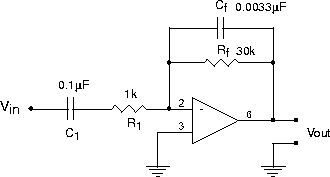
To make a high gain amplifier with a fairly narrow bandwidth, we cascade three (3) identical stages. The gain is then:
|
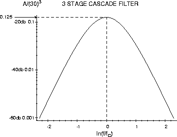
How does the frequency of peak gain compare to your calculated
f°?
(For the input signal, use the 100 × attenuator on the wave-form
generator output). Measure
the input and output voltage with a scope, not the DVM.
You can use the
DVM if you are careful to take the noise into account.
How do you do this?