pn Junctions
Murray Thompson
Sept. 13, 1999
1 Introduction
This is a non-rigorous explanation to give you an understanding of the
background for the operation of semiconductor diodes and the Diode Equation.
This explanation is intended to fill in part of the missing background in H& H.
We advise 623 students to read R.E. Simpson's book
``Introductory Electronics for Scientists and Engineers'' pages 162 - 185.
Since this explanation is an addition to the lectures in which pn junctions
are discussed, it assumes some of the material from the 623 lectures plus some material from the
other physics courses and is not intended
to be a full explanation of pn junctions.
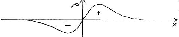
2 Multiple One Dimensional Potential Wells
In Quantum Mechanics, we learn how the wavefunctions of the electrons which are
held in a potential well such as an atom are eigenfunctions and must satisfy
the boundary conditions. In an artificial but more easily understood
one-dimensional situation, these boundaries are on the left and right.
Suppose we have found an eigenfunction with an energy eigenvalue
E for a one dimensional potential well.
Now consider 2 such wells side by side.
We find that now at energies near E, we have 2 eigenfunctions.
Similarly, if 3 wells are placed side by side, we have 3 eigenfunctions.
If N wells are placed side by side, we have N eigenfunctions with close
values of E.
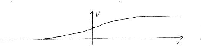
3 Multiple Three Dimensional Potential Wells
Although it is not practical to draw the 3D potential wells and eigenfunctions,
we find that N wells again give N different solutions or eigenfunctions
with N slightly different energy eigenvalues. These fit within a band of
energies with the
lowest being that for the eigenfunction with fewest crossings of
Y = 0 and
highest being that for the eigenfunction with most crossings of
Y = 0.
In any object which can be seen, the number N of wells (number of atoms) is
extremely high since Avogadro's Number is
NA = 6.024×10²³ atoms/mole.
Thus in any object which can be seen, the energies occupy a band in a virtually
continuous way.
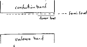
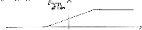
4 Fermi Level
The ``Fermi Level'' in a crystal is the highest energy level of electrons
when the crystal is at a temperature of absolute zero (0° K).
Pure Si and Ge crystals act as insulators.
5 Semiconductors
Semiconductors are materials which would have been insulators except that a
very tiny fraction of particular impurities has been added.
These impurities are called dopants and can have an enormous effect.
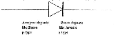
6 p Type and n Type Materials
A crystal such as silicon can have two types of impurity atoms (dopants)
which are infused with very low concentrations which, however, can have
very significant effects. These impurities give two types of doped materials,
``p type'' and ``n type'' which we describe below and,
for simplicity in most diagrams, we will place p type with acceptor dopants
on the left and n type with donor dopants on the right.
7 Donor Levels in n type Material
Consider the doping of a Silicon (ZSi = 14) crystal with a few atoms of
Phosphorus (ZP = 15).
Phosphorus has 5 valence electrons.
(Arsenic ZAs = 33 or Antimony ZSb = 51 are similar.)
Each Phosphorus
atom sits among Si atoms and Si covalent bonds so that the 5th electron of
each P atom is very loosely held. It is said to be in a ``donor'' level.
Its wavefunction has an energy eigenvalue
which is well above those of the bonded electrons and is close to the
conduction levels.
When the electron moves away from its original donor atom,
the donor atom is left with positive charge (it now has 4 electrons instead
of 5) (qdonor = +e = +1.602×10⁻¹⁹C)
and so the negative electron is weakly held by the single
positive charge of the remaining donor nucleus and
electrons.
The electron (-) and its donor atom (+) form an ``atom'' with a positive
nucleus and a negative electron moving about it. The electron sees a potential well
V(r) = -[e.e/( 4per)]
where
e = erelativee0 and erelative
is the relative permittivity of silicon
erelative » 12.
Whereas in the case of Hydrogen, the binding energy of the electron,
in the ground state to the proton is
EB = -[(melectrone4)/( 2(2e0h)2)] = -13.6 eV,
the binding energy of the electron to the donor atom is
EB = -[(melectrone4)/( 2(2erelativee0h)2)] » 0.1 eV
and has an
energy level or ``donor level'' close below the conduction band.
Since there are many of these ``donor atoms'', the n type material has many
such states with the donor energy levels forming a diffuse band.
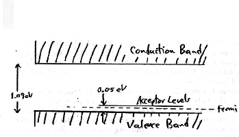
The typical donor level is only about 0.05 eV below the
conduction band and 1.04 eV above the valence band and the eigenvalues of
the bonded electrons.
The donor eigenstate can be thought of as a disturbed valence state. If the
temperature is lowered to 0° K, then the electron in the donor level cannot
fall to a lower state since all the other valence states are full.
Thus the Fermi Level must lie above the donor level but below the
conduction level.
The electron carriers have an energy level or ``donor level'' close under the
conduction band (typically 0.050 eV below the conduction band).
At normal temperatures (at 300° K, kT=0.026 eV), a large fraction of these
electrons can lift into the conduction band and move freely about the crystal.
Such freely moving ``left over electrons'' then exist in a field with most
of the crystal being neutral but the donor atoms being randomly scattered
positive (qdonor = +e = +1.602×10⁻¹⁹C) charges and of course the other
negative ``left over electrons'' making the combination neutral.
8 Electrons and Holes
Holes are found in p type material with ``acceptor atoms''.
Acceptor atoms, such as Boron (ZB = 5), Indium (ZIn = 49),
Gallium (ZGa = 31) and
Aluminum (ZAl = 13), have 3 valence electrons rather than 4
like silicon (ZSi = 14) or Germanium (ZGe = 32).
At each acceptor atom in a Silicon crystal,
3 electrons are bound in covalent bonds to the 4
adjacent Si atoms but 1 electron is ``missing'' and we say this incomplete
bond has a ``hole''.
The hole can be exchanged with adjacent bonds by the electron of the bond
being taken and put into the hole to complete its bond.
Thus, a hole can be moved about from bond to bond (robbing Peter to pay Paul).
(This can be compared with moving a car from one slot in a parking lot to the
only other available empty slot. The effect is the same as moving the empty slot
from the second place to the first. The empty slot can be moved all around the
parking lot and is similar to the hole being moved all around the crystal.)
The electrons are equivalent to the cars and the holes are equivalent to the
empty slots.
Both the mobile electrons and the mobile holes carry charge (+e and -e )
and are referred to as ``carriers''.
Both p type and n type have both kinds of carriers but the p type has a
majority of hole carriers while the n type has a majority of electron carriers.
9 Acceptor Levels in p type Material
The quantum mechanics for the ``hole'' in p type material
has an equation like that of an electron.
The hole has an effective mass, which is a little greater than the
electron mass, and has a positive charge (q=+e).
When the hole moves away from its original acceptor atom,
the acceptor atom is left with negative charge (it now has 4 electrons instead
of 3) (qacceptor = -e = -1.602×10⁻¹⁹C)
and so the positive hole is weakly held by the single
negative charge of the remaining acceptor nucleus and
electrons.
The hole (+) and its acceptor atom (-) form an ``atom'' with a negative
nucleus and a positive hole moving about it. The hole sees a potential well
V(r) = -[e.e/( 4per)]
where
e = erelativee0 and erelative
is the relative permittivity of silicon
erelative » 12.
As before, the binding energy of the hole to the acceptor atom is
EB = -[(mholee4)/( 2(2erelativee0h)2)] » 0.1 eV
and has an energy level or ``acceptor level'' close above the valence band.
Since there are many of these ``acceptor atoms'', the p type material has many
such states with the acceptor energy levels forming a diffuse band.
The acceptor eigenstate can be thought of as a disturbed conduction state. If the
temperature is lowered to 0 K, then each electron in the acceptor level
falls to fill all empty valence states and the acceptor states are ocupied
by holes.
Thus the Fermi Level must lie below the acceptor level but above the
valence level.
At normal temperatures (at 300° K, kT=0.026 eV), a fraction of these
holes can fall into the valence band (ie the electrons lift from Valence to
Conduction bands) and these holes move freely about the crystal.
Such freely moving ``holes'' then exist in a field with most
of the crystal being neutral but the acceptor atoms being randomly scattered
negative (qacceptor = -e = -1.602×10⁻¹⁹C charges and of course the other
positive ``holes'' making the combination neutral.
10 Adjacent p and n Type material
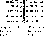
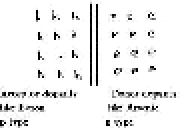
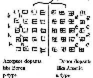
Consider two semiconductors which are p-type on the left and n-type on the right
and which are not in contact.
First draw the Acceptor atoms in the p-type material on the left and
draw the donor atoms in the n-type material on the right.
We ignore the very much more plentiful and more regularly
placed neutral Silicon atoms.
We draw the acceptor atoms such as B, In or Al (which are fixed
in place in the p-type crystal) on the left
and draw the donor atoms such as P, As or Sb (which are fixed
in place in the n-type crystal) on the right.
We draw acceptor atoms as small squares and
donor atoms as small squares
with their residual charge after they have accepted the extra electron or
donated one of their electrons.
Although the acceptor and donor atoms are drawn here in a fairly regular array
for a simple drawing, the acceptor and donor atoms are dopants of the crystals
and are really distributed in a fixed but random and statistically smooth manner
Now draw the two materials with the surrounding holes h (missing
electrons) and extra electrons
e.
While these h and e have been drawn in particular positions,
they are really diffusing and moving about.
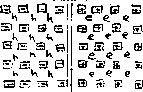
Remember that the Silicon atoms, acceptor atoms and donor atoms are fixed
in the lattice by their remaining 3 or 4 covalent bonds/atom and cannot move.
They provide a relatively neutrally charged medium plus a few positively
or negatively charged stationary centers.
The few h's and e's move in this medium and are called the ``carriers''.
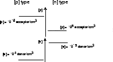
The following 2 graphs show, on a vertical logarithmic scale, some typical hole
(p) and electron (e) carrier densities in p-type material on the left and
n-type material on the right.
Notice that the both of the products of the p n densities on the two sides is
the same pn = 1020acceptor/cm3.donor/cm3
due to the law of mass-action and
a tiny fraction of e carriers exist even in p-type material and
a tiny fraction of hs or (p) carriers exist even in n-type material.
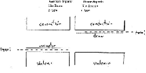
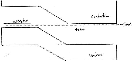
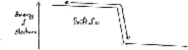
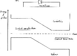
The following two sketches, side by side, show the empty conduction and full
valence bands for the two untouching materials.
11 p and n Types in Contact
NOW LET THE TWO MATERIALS BECOME IN CONTACT
Again draw the two materials with the surrounding holes h and electrons
e.
The holes and electrons near the boundary will diffuse into the
adjacent material
and most of these will recombine.
This will leave the boundary with very few free carriers.
We call this region a ``Depletion Layer''.
The charge density (due mostly to the unbalanced charges at
Acceptor atoms and Donor atoms)
will have a graph of
r = qe(p - n + Ndonor - Nacceptor):
The actual direction of the Electric field [E\vec] due to these unbalanced
charges will be from right to left ¬. The x components will
be
[(Ex)\vec] = [1/( 4pe)]ň-Ąx r(x)dx
We write the electric field as a vector [E\vec] to distinguish it from the
later energy E of each electron.
If we graph the magnitude of the [E\vec] in the [(+x)\vec]
direction, we will have a negative [(Ex)\vec].

We can get V from V = -ň-Ąx[E\vec].[dx\vec]:
Thus, the simple joining of the p and n type materials (actually grown together)
has caused two surprising effects.
- two charges have appeared near the joining surface - negative in the
p type and positive in the n type.
- A potential barrier V and an associated electric field [(Ex)\vec]
have appeared with [(Ex)\vec] having a direction from n type to p type
pushing holes from n type into p type
(from the right to the left in our diagrams).
The Energy of the holes is +e×(the electric Potential V) where e is
the elementary charge e = +1.602×10⁻¹⁹C, and so for our
left p type and right n type appears similar to that of the Electric Potential.
Similarly, we can draw the energy of the electrons (with an inversion due to
the electrons having negative charge -e) and,
this leads to the energy bands of the electrons.
By placing the 2 materials in contact, they form a pn junction diode
with the symbol matching the left to right p type to n type.)
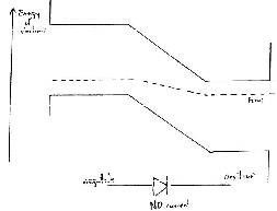
AFTER A SHORT TIME WE WILL HAVE EQUILIBRIUM
Even though we have NOT YET applied an external voltage,
the existence of the charged donor and acceptor atoms,
with their hs and es,
creates an electric field across the junction which retards and prevents
further net carrier movement.
On both sides of the junction we will have a region which is
nearly empty of carriers.
This is called the Depletion Region.
Actually, of course, the carriers still move a little
but the net movement becomes zero.
We define two kinds of origins for electron movement.
- Drift = movement due to Electric Field
The movement is not infinite because the electrons are scattered especially
when as each electron accelerates, the de Broglie
l = h/p
of the electron momentum becomes comparable with the atomic diameter and the
electron is likely to be scattered.
Thus the x component of its velocity rises as it accelerates then falls to zero
and the acceleration starts over again.
Thus the average speed of the electron is limited.
- Diffusion = movement due to a concentration gradient and range of energies
The diffusion flow is proportional to the product of
(concentration)×
(the fraction of carriers which have sufficient energy to overcome any
potential barrier E-Ef)
where Ef is the Fermi Energy and E is greater than Ef.
The electrons and holes are fermions and therefore have energy distributions
which obey the Fermi-Dirac statistics.
f(E) = [1/( e(E-Ef)/kT + 1)]
where k is Boltzmann's Constant.
If the barrier E is increased, fewer electrons will be able to diffuse past
the barrier and so f(E) is decreased.
At normal temperatures, this distribution f(E)
cannot be distinguished from the Boltzmann distribution.
f(E) = [1/( e(E-Ef)/kT)]
The distribution of energies does not have the sharp cutoff found at low
temperatures but a few have higher energies.

For example, considering the electron carriers,
if the density is n electron carriers/unit volume, and they encounter an
energy barrier
with height E0 = -eV0 against the electrons moving
from n type on the right to p type on the left,
the number of electron carriers/second which can diffuse from n type to p type
past the barrier due to the temperature T will be proportional to
Rate µ ne(-E+Ef )/kT
Rate µ ne(-eV0 )/kT
Rate µ = n e-([(eV0)/ kT])
where T is the absolute temperature, and k is Boltzmann's constant.
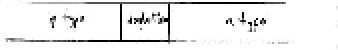
Acceptor dopants Donor dopants
like Boron like Arsenic
p type n type
Note that in the equation, the first e = 2.7182818 while the second
e = 1.602192×10⁻¹⁹C where the electron carries the charge of
``-e''. It is hard to avoid this duplication but it
seldom causes confusion.
Consider the combined Drift + Diffusion.
- For the electrons in equilibrium (p type atoms on left, n type atoms on right);
With NO applied voltage, we have NO total current and so:
Drift of es due to the Electric Field =
- Diffusion of es due to the Concentration gradient
- For the holes in equilibrium (p type atoms on left, n type atoms on right);
Similarly, with NO applied voltage, we have NO total current and so:
Drift of hs due to the Electric Field =
- Diffusion of hs due to the Concentration gradient
Thus, in equilibrium,
Combined Drift = - Diffusion µ - n e-([(eV0)/ kT])
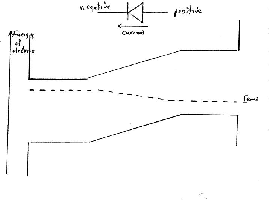
12 Now Raise the voltage of the p Type by V
NOW APPLY A VOLTAGE V ACROSS THE TWO MATERIALS
We make the left p type material have a voltage V relative to the right
n type material.

- If V is positive with the p type material on the left having a voltage above
that of the n type material on the right, it is to be expected that this
voltage will cause the holes on the
left to drift to the right and the electrons to drift to the left.
The moving hs and es will intermingle and cancel each other. The movement
of the charges will be an electrical current.
-
If V is negative, then the holes and electrons will be drawn slightly further
apart until the junction field is increased and the movement stops.
Except for the brief slight movement, no charges move and so there is
no current.
While these effects are easy to understand, we want to get some algebra to
describe the size of the current as a function of the voltage V causing it.
The raising of the voltage on the left (p type atoms) will lower the energy
of the electrons on the left and will lower the
energy barrier E = eV0 against the electrons moving to the left
is changed from eV0 to e(V0-V).
- Drift
The combined drift due to the electric field is unchanged
because, if the barrier is abrupt,
the voltage height of the barrier does not affect
the number of carriers which drift over it.
- While some distance from the abrupt drop and where the potential slope is
gentle, the drift is proportional to the applied Electric Field
Flow µ -eEx.
- However, once an electron starts to fall over the potential drop, it
will continue regardless of the potential or height.
(An analogy of rate of water flow in a river towards and over a dam may help.
In the river, the water flow (in meter3/second) is dependent
upon the slope of the river since the removal of any volume
of water will make
the water behind it flow faster. However the water flow over the dam is
independent of the height of the dam if the fall
is abrupt since,
once any volume of water has fallen over the edge, the absence of that volume
of water does not cause less water to flow even if the dam height is
reduced significantly.)
® Drift of es
Acceptor dopants Donor dopants
like Boron like Arsenic
p type n type
-
Diffusion
The combined electron and hole diffusion to the left,
due to the concentration gradient, past the barrier
due depends upon the temperature and barrier height and becomes
diffusion µ e-([(e(V0-V))/ kT])
Since the voltage height of the barrier between the two materials
does not effect the number of carriers which drift over it,
the NET rate of flow of carriers ``over'' the potential drop is given by the
following equation with the ``drift'' component unchanged.
Net Flow µ [diffusion + drift]
Net Flow µ [e-([(e(V0-V))/ kT]) - e-([(eV0)/ kT])]
Net Flow µ e-([(eV0)/ kT])[e([eV/ kT])-1]
The resulting current is
I µ e×(NET Flow)
I µ e×e-([(eV0)/ kT])[e([eV/ kT])-1]
We combine the proportionality constant, the value of the elementary charge
e = 1.602×10⁻¹⁹C on
each electron and hole and the first term
e-([(eV0)/ kT]) into a constant ``saturation current''
Is µ e×e-[(eV0)/ kT] to
get the electric current
I = Is [e([eV/ kT])-1]
Diode Equation or Ebers Moll Equation. (H&H pg 80)
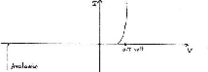
Graph of (Voltage of p type on left relative to n type on right)
versus I
Notes
- The voltage at which significant conduction occurs is about 0.7 V
for Si and about 0.4 V for Ge.
(Of course, the definition of ``significant current'' will depend upon
the application. In an application with very small currents (in mA),
one might say the the forward conduction voltages are about 0.6 V for
silicon and 0.3 V for Ge.)
- If the voltage is reversed, the current becomes even small and the
depletion region is nearly completely exhausted of charge carriers.
However, if the voltage is made even more negative, then the electric field
within the narrow depletion zone can become sufficiently high for avalanche
effects to occur.
In an avalanche, a stray electron (perhaps produced by the ionization trail of
a cosmic ray can accelerate so rapidly that it may not be scattered when its
de Broglie wavelength is comparable with a nearby atomic potential well and it
may gain enough energy that, when it eventually hits an atom,
it may ionize the atom.
The 1 electron may cause 2 loose electrons which, in turn, cause many more.
Thus at a critical large reverse bias, the current may increase suddenly.
This effect is used in Zener Diodes.
- The constant term Is is dependent upon the geometry and the
doping but is usually very small.
If we measure current in mA or Amp and voltage in mV, the exponential term is
also small until V reaches about 0.7 V. Then, because for
each increment of 0.026 V,
the exponential term grows by a factor of e = 2.718 and for each
increment of 0.26 V,
the exponential term grows by a factor of e10 = 2.71810 = 22,000 and the
graph of V versus I shows a sudden climb.
For example, if Is = 10-13A = 10-10mA = 100pA then
I = Is [e([eV/ kT])-1]
can be calculated with I in mA;
|
|
| V | e[V/ 0.026 Volt] | I = 10-13A [e([eV/ kT])-1]
|
| | I = 10-10mA [e([eV/ kT])-1] |
|
|
| 0.0 Volt | 0.00 | 0 mA
|
| 0.1 Volt | 3.85 | 0 mA
|
| 0.2 Volt | 7.69 | 0 mA
|
| 0.3 Volt | 11.54 | 0 mA
|
| 0.4 Volt | 15.38 | 0 mA
|
| 0.5 Volt | 19.23 | 0 mA
|
| 0.6 Volt | 23.07 | 1 mA
|
| 0.7 Volt | 26.92 | 49 mA
|
| 0.8 Volt | 30.77 | 2,306 mA
|
| 0.9 Volt | 34.63 | 107,962 mA
|
| 1.0 Volt | 38.46 | 5,053,984 mA |
Since current I is so tiny below about 0.7 V and climbs so sharply above
0.7 V, the graph of the equation is often thought of as a horizontal line and
a vertical line.
Since at high reverse voltages, an avalanche effect can be caused in the
junction, the current can begin abruptly if the reverse voltage is increased
to much. This can possibly destroy the diode but is actually intended in some
diodes, where another component limits the current.
Thus, in general, the oversimplified voltage current characteristic of a
pn junction has 1 horizontal line and 2 vertical lines.
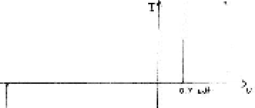
Oversimplified graph for pn junction of
V (of p-type on left relative to n-type on right) versus I
13 Dynamic Resistance of the PN Junction
- Define the ``Dynamic Resistance'' as the effective resistance for small
changes with definition rtr = [dV/ dI]
The Diode Equation is I = Is [e([eV/ kT])-1].
Differentiate this equation for the diode current I with respect to V.
[1/( rtr)] = [dI/ dV] = [e/ kT] Is [e([eV/ kT])] » [e/ kT] I since eV >> kT and so e[eV/ kT] >> 1
Thus the ``junction dynamic resistance'' or ``transresistance''
of the junction is
rtr = [dV/ dI] = [kT/ eI] = [0.026 electron volt/ eI] = [0.026 volt/ I] where I is measured in Amps.
For example, if a silicon diode passes a current of 1 milliamp
junction Dynamic resistance = rtr » [0.026 volt/ 0.001 Amp] = 26 ohms.
-
In addition, the materials add a little ohmic resistance as well, typically
about 2 ohm (depending upon the physical size of the material).
Thus the total dynamic resistance of a Silicon diode is typically about
Rdynamic = rtr = [dV/ dI] = 2 ohm + [0.026 volt/ I]
or
Rdynamic = rtr = [dV/ dI] = 2 ohm + [(0.026 ohm/Amp)/ I]
[This is sometimes expressed poorly (please do not do this)
with inconsistent units as
Rdynamic = [dV/ dI] = 2 ohm + [26/( ImA)] ]
The added 2 ohms is typical but will vary from diode to diode
depending upon the diode width and construction.
For example, if I = 10 mA, then
Rdynamic = rtr = 2 ohm + [(0.026 ohm/Amp)/ 0.010 Amp]
Rdynamic = rtr = (2+ 2.6) ohm = 4.6 ohms.
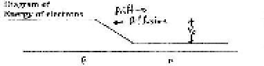
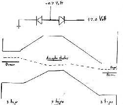
14 Energy Levels in Junctions
- Unbiased Junction (no voltage applied)
(p type with acceptor impurity atoms on left and n type with donor
impurity atoms on right)
Acceptor dopants Donor dopants
like Boron like Arsenic
p type n type
- This is not drawn to scale!
- The band gap is about 1.09 eV to 1.12 eV for Silicon
- The ionized acceptor states are only about 0.05 eV above the valence band.
- the Fermi level is only about 0.025 eV above the valence band.
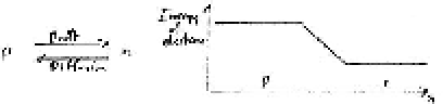
- Forward-Biased Junction
(Positive voltage applied to p type material on left).
(p type with acceptor impurity atoms on left and n type with donor
impurity atoms on right)

Acceptor dopants Donor dopants
like Boron like Arsenic
p type n type
- When forward biased, many of both kinds of mobile carriers are drawn
into the junction region eliminating the charge depletion.
The holes are not filled immediately by electrons and we say the region has a
storage charge.
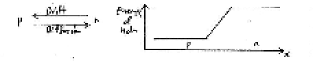
- Back-Biased Junction
(Negative voltage applied to p type material)
(p type on left and n type on right)
Acceptor dopants Donor dopants
like Boron like Arsenic
p type n type
- When back biased, all mobile carriers are drawn away from the junction
region causing a wider charge depletion region.
- Mirror Image of Forward-Biased Junction
(Positive voltage applied to p type material on right.)
(p type with acceptor impurity atoms on right and n type with donor
impurity atoms on left.)
To make a later diagram more easy to understand, we have drawn here a simple
reflection (left/right) of the earlier Forward-Biased Junction diagram.
15 Two pn Junctions
- Combination of Forward-Biased Junction and Back-Biased Junction
Consider a crude ``npn junction transistor'' as two pn junctions joined with
a common ``base'' of p type material.
Apply a positive voltage to the middle p type material with respect
to the n type ``base'' material on the left and apply a positive voltage of
about +2.0 V other n type material on the right.
This can be looked upon as the combination of the above examples 3 and 4.
The voltage applied to the middle p type (relative to the left n type) must
be close to 0.7 V so that the left junction conducts a noticeable current.
Temporarily consider a pair of pn diodes coupled so that the p type materials are joined.
Apply voltages so that the left np junction is forward biased (ie conducting)
and the right pn junction is back biased (ie NOT conducting).
- Combination of Forward-Biased Junction and Back-Biased Junction
with Narrow Middle and a Higher Back-bias
This is now close to becoming an npn ``junction transistor''.
Apply a positive 0.7 V to the middle p type material with respect
to the n type ``base'' material on left and apply a larger positive voltage
of about +20 V to other n type material on the right.
The terminals are given names:
emitter: the left n type material
base: the very thin middle p type material
collector: the right n type material.
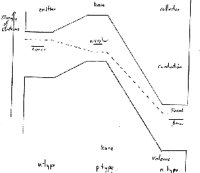
16 An npn Junction Transistor
A real npn junction transistor has a very thin base so that electrons
leaving the
emitter and travelling into the base immediately ``feel'' the strong electric
field [E\vec] of the back-biassed junction and can fall ``downhill towards
the collector''.
By making the base thin, the chance of the electrons meeting a free hole
in the p type base before being swept away by the collector's field can be
reduced to about 2% in spite of the high concentration of holes in the p type
base. In other words, if a current i leaves the emitter,
then only about 0.02 i leaves the base wire and about 0.98 i leaves the
collector.
The fraction which leaves the base wire is called a.
a = [(ibase)/( iemitter)]
In this example
a = [0.98/ 1.0] = 0.98
The ratio of the current which
leaves the collector to that which leaves the emitter is called b.
b = [(icollector)/( ibase)]
In this example,
b = [0.98/ 0.02] » 49.0
File translated from TEX by TTH, version 1.93.
On 20 Sep 1999, 15:23.