The first step in this experiment is to measure and record the common emitter characteristic curves for a silicon NPN 2N1480 transistor. These are diffused junction transistors with a fairly small base current gain.
- Your lab instructor will illustrate the basic principles of operation of the Fairchild 6200 curve tracer and you will then photograph the resulting curves.
- Be sure to record the appropriate scale readings for your transistor for later analysis. Note also the wide variation between your transistor and those of your neighbors. In the Appendix we give the specifications for this transistor as listed by the manufacturer.
- Compare your measured b (b is sometimes called hfe on the spec sheet) to the range given on the spec sheet.
So far we have been concerned only with the properties of the transistor itself. In practical amplifier applications, it is desirable to design a circuit whose properties are predictable, ie which don't depend strongly on your accidental choice of a specific transistor. In Fig. 1 we show a very common configuration of base and emitter biasing for the common emitter configuration of amplifier. This circuit is reasonably stable against variations in transistor properties (for b = hfe ranging from 14 to 40, the Q point stays within 20% of VCE @ 6.5 V).

- Construct the Thevenin equivalent circuit for the base bias circuit.
-
The base-emitter voltage drop for a turned on Si transistor is 0.6 V. Therefore
VE = VB - 0.6 V -
The emitter current IE, will be IE = [(VE)/(RE)] from Ohm's law. The base current IB = [(IE)/(b)]. You can load your Thevenin equivalent of the base bias circuit with the current IB and calculate a new VB. You could solve these equations simultaneously to get the exact operating point, but this is seldom necessary. If the design is good (meaning not too sensitive to b, a single iteration will yield a very accurate approximation to the operating point.
- Using Ohm's law, calculate IE, and, thus IC, since they are about the same.
-
From the equation for the collector-emitter circuit:
VCC = IC RC + VCE + IE RE IC = (VCC - VCE)
(RE + RC)
- the input impedance (ri),
- the output impedance (ro) and
- the voltage gain (Av = vo/vi).
Before actually measuring these quantities, it is enlightening to estimate them.
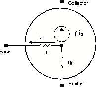
Use the transresistance model, in which the transistor is replaced by an equivalent circuit containing a current generator ic = bib in series with the base emitter resistor rtr (called the transresistance). The equivalent circuit is shown in Fig. 2. By differentiating the basic diode equation (for a p-n junction), it has been shown in class that the dynamic base emitter resistance or ``transresistance'' is inversely proportional to the current IE.
rtr = [(¶V)/( ¶I)] = [(0.026 ohm/A)/(Ie)].
[This is commonly expressed in mixed non-SI units by measuring IE in milliamps IE(mA) and expressing the ratio as; ``rtr = [26/(IE(mA))]''. However, we prefer you to avoid this expression and use the normal equations given above and below with consistent SI units as rtr = [(0.026 ohm/A)/(IE)] which is the same as
rtr = [0.026 volt/(IE)].]
Thus, the transresistance is:
|
where we have assumed IC @ IE and the ``2 ohm'' is a rough average value for the ohmic resistance (rb) between the lead and the base emitter junction. Note that an AC signal introduced on the base lead can pass to AC ground through three paths, R1, R2, and through the transistor. So, ri (input impedance) is calculated (with ``||'' meaning ``in parallel'' so you add reciprocals to get the reciprocal of the combination) as:
|
|
- Now introduce a AC signal (a sine wave from the waveform generator) of frequency f = 5 KHz into the base through a coupling capacitor Cc ł 1.0 mF and measure ri, Av and ro. To measure ri , introduce a series resistor (R3), and calculate ri using the voltage divider equations.
- Vary the magnitude of the input signal and note any distortion in the output signal which results.
- Interpret the distortion using the output characteristics and the load line.
- Measure the frequency response (or band width) of your amplifier (Av(w)) and try to identify the lower corner frequency in terms of the component values.
- Connect a 1 to 2 mF capacitor across RE and remeasure ri,
ro
and Av. Again use the transresistance model to estimate the voltage gain
and compare to your measurements. Note: The input signal must be reduced
in magnitude by a factor ~ 20 - 50, which can be accomplished using the
attenuator provided.
- Verify the reduction and connection at the input to the amplifier using the scope.
Note the increased gain (and also the smaller bandwidth compared to the circuit incorporating feedback. The distortion is due to the fact that we are supplying the transistor with a voltage signal, whereas transistors are primarily current amplifiers. - To produce a current signal for the input, introduce a 50k resistor in series with the function generator output to produce a high impedance (current) source.
- Note that now vo is undistorted while vbe is considerably distorted. Try to interpret this effect in your report.